Thin wafer market by Process (Temporary Bonding & Debonding and Carrier-Less Approach), By Application (MEMS, CIS, Memory, RF Devices, LED, Interposers, Logic, and Others), By Wafer Size (125MM, 200MM, and 300MM), By Technology (Wafer Grinding, Wafer Polishing, and Wafer Dicing) and By Region – Global Opportunities & Forecast, 2022-2029
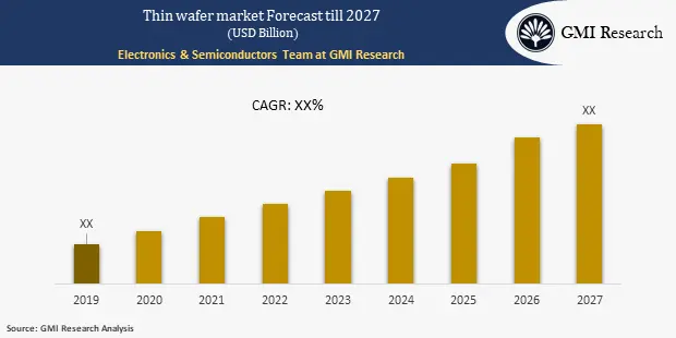
Thin Wafer Market is estimated to grow at a robust CAGR during the forecast period 2022-2029

To have an edge over the competition by knowing the market dynamics and current trends of “Thin wafer market,” request for Sample Report here
Key Drivers
The global thin wafer market is projected to witness strong demand during the forecast period. The accelerating adoption of MEMS technology in portable health monitoring devices, along with the decreasing size of electronic devices, are the two significant factors that are contributing to the growth of the market in the coming years. Moreover, the increasing number of smartphone and consumer electronics and high amount of material saving are further surging the growth of the market. With the strong demand for telecommunication systems, driven by the growing emphasis on e-learning, is another factor that will open new doors for market growth. In addition to this, the demand for MEMS is surging due to its increasing adoption such as in portable medical devices, automotive sensor devices, and communication systems. The miniature design of the MEMS enables it to be used in almost every electronic devices, which in turn, is boosting the demand for MEMS in the semiconductor market.
The leading vendors are focusing on satisfying the accelerating requirement of memory disks, wireless devices, and consumer electronics. The thin wafers have the ability to deploy the management of thermal and electronic devices, which is anticipated to propel the demand of the market in the coming years. The ultra-thin wafer is more volatile and susceptible to damage user stress or cracking. Furthermore, the increasing applications of the thin-wafers, such as in power devices, advanced packaging applications, LEDs, and RF devices, will enhance the growth of the market. One of the biggest issues faced by organizations is the lower efficiency of the thin wafers. A thin wafer has light absorption capacity for long wavelengths, particularly in case if the thickness is below 50 mm. Moreover, with the outbreak of the COVID-19, there are delays in the investment plans related to the capacity expansion by the wafer manufacturers. This factor will have a negative impact on the growing demand of the market, especially in 2020.
Do you want to know more about the Research process and detailed Methodology, Request Research Methodology of this report
Wafer Size – Segment Analysis
Based on the wafer size, 300 mm wafer segment is anticipated to grow at a higher CAGR during the forecast period. The increasing usage of 300 mm in LEDs driven by the ability of these wafers to provide greater yield, is a significant factor that is energizing the growth of the segment in the market. It is becoming essential for the leading LED manufacturers to achieve economies of scale and enhance their profitability, which is offered by these wafers. In addition to this, the rising number of operational 300 mm wafer fabrication facilities is another factor that is contributing to the growth of the market.
Technology – Segment Analysis
On the basis of technology, the wafer dicing segment is projected to witness a faster CAGR over the forecast period. This is mainly due to the strong demand for high-speed dicing and superior breakage strength. Additionally, the need for smaller, higher performing, and lower cost device configuration for the use in various devices, such as in logic devices, power devices, sensors, and memory devices, is further energizing the demand of the segment in the market.
Application – Segment Analysis
Based on the Application, the LED segment is predicted to lead the market during the forecast period. This is attributed to the increasing applications of thin wafer in the LED as it helps in increasing the profitability of the manufacturers. The thin wafer is being widely used in LEDs to develop a variety of electronic products and its components.
In case, any of your pain points areas are not covered in the current scope of this report, Request for Free Customization here
Regional – Segment Analysis
Based on the region, Asia-pacific region is expected to dominate the market during the forecast period owing to the increasing adoption of high-end consumer electronics, including smart home devices and wearables, particularly in Japan and China. In addition to this, the increasing number of investments and continuous expansion in the businesses in the Asian countries is further opening new doors for the growth of the market in this region. For instance, in 2019, Samsung Corporation invested USD 111 billion, with an aim to expand its Memory and Foundry businesses in the next 10 years. Furthermore, the semiconductor market in this region is growing at a significant rate owing to the favorable economic conditions and the strong demand for consumer electronics. The combination of these factors is contributing to the growth of the market in this region.
Top Market Players
Various notable players operating in the market include SK Siltron Co., Ltd., Shin-Etsu Chemical Co., Ltd., Siltronic, SUMCO CORPORATION, Globalwafers Co. Ltd., Lintec Corporation, DISCO Corporation, 3M, Applied Materials, Inc., and Nissan Chemical Corporation, among others.
Key Developments:
-
- In 2020, Siltronic, announced to invest in epitaxial reactor to improve its production capacity of GAN-on-Si wafers portfolio in response to the surging demand for such wafers in applications such as data centers and 5G networks. The GAN technology supports the efficient energy distribution under high power densities.
- In 2020, SK siltron Co.,Ltd., acquired the DuPont’s Silicon Carbide Wafer unit. Through this $450 Million acquisition, the company aims to capture the growing demand from consumers and government bodies for sustainable energy and environmental solutions.
- In February 2020, GlobalWafers Co., Ltd. and GLOBALFOUNDRIES (US), the world’s leading specialty foundry, signed a memorandum of understanding (MOU) to develop a long-term supply agreement for 300 mm SOI wafers. The agreement is projected to strengthen its 300-mm SOI wafer manufacturing capabilities.
Segments covered in the Report:
The global thin wafer market has been segmented on the basis of Process, application, Wafer Size, Technology and key regions. Based on process, the market is segmented into temporary bonding & debonding and carrier-less approach. The temporary bonding & debonding segment is further segmented into UV-release adhesives, thermal-release adhesives, and solvent-release adhesives. Based on application, the market is segmented into MEMS, CIS, memory, RF devices, LED, interposers, logic, and others. Based on wafer size, the market is segmented into 125MM, 200MM, and 300MM. Based on Technology the market is segmented into wafer grinding, wafer polishing, and wafer dicing.
For detailed scope of the “Thin wafer market” report request a Sample Copy of the report
Key questions answered in this research report:
-
- At what pace is global thin wafer market growing? What will be the growth trend in the future?
- What are the key drivers and restraints in thin wafer market? What will be the impact of drivers and restraints in the future?
- What are the regional revenues and forecast breakdowns? Which are the major regional revenue pockets for growth in the global thin wafer market?
- Which technology generated maximum revenues in 2021 and identify the most promising technologies during the forecast period?
- What are the various application areas of global thin wafer market and how they are poised to grow?
- What companies are the major participants in this market and their business strategies, how does the competitive landscape look like?
|
Report Coverage |
Details |
| Market Revenues Currency |
USD Billion |
| Market Base Year |
2021 |
| Market Forecast Period |
2022-2029 |
| Base Year & Forecast Units |
Revenues (USD Billion) |
| Market Segment | By Process, By Application, By Wafer Size, By Technology, By Region |
| Regional Coverage | Asia Pacific, Europe, North America, and RoW |
| Companies Profiled | SK Siltron Co., Ltd., Shin-Etsu Chemical Co., Ltd., Siltronic, SUMCO CORPORATION, Globalwafers Co. Ltd., Lintec Corporation, DISCO Corporation, 3M, Applied Materials, Nissan Chemical Corporation, among others; a total of 10 companies covered. |
| 25% Free Customization Available | We will customize this report up to 25% as a free customization to address our client’s specific requirements |
Market Segmentation
Global Thin wafer market by Process
-
- Temporary Bonding & Debonding
- UV-Release Adhesives
- Thermal-Release Adhesives
- Solvent-Release Adhesives
- Carrier-less Approach (Taiko Process)
- Temporary Bonding & Debonding
Global Thin wafer market by Application
-
- MEMS
- CIS
- Memory
- RF Devices
- LED
- Interposers
- Logic
- Others
Global Thin wafer market by Wafer Size
-
- 125 mm
- 200 mm
- 300 mm
Global Thin wafer market by Technology
-
- Wafer Grinding
- Wafer Polishing
- Wafer Dicing
Global Thin wafer market by Region
-
- North America Thin wafer market (Option 1: As a part of the free 25% customization)
- By Process
- By Application
- By Wafer Size
- By Technology
- US market All-Up
- Canada market All-Up
- Europe Thin wafer market (Option 2: As a part of the free 25% customization)
- By Process
- By Application
- By Wafer Size
- By Technology
- UK market All-Up
- Germany market All-Up
- France market All-Up
- Spain market All-Up
- Rest of Europe market All-Up
- Asia-Pacific Thin wafer market (Option 3: As a part of the free 25% customization)
- By Process
- By Application
- By Wafer Size
- By Technology
- China market All-Up
- India market All-Up
- Japan market All-Up
- Rest of APAC market All-Up
- RoW Thin wafer market (Option 4: As a part of the free 25% customization)
- By Process
- By Application
- By Wafer Size
- By Technology
- Brazil market All-Up
- South Africa market All-Up
- Saudi Arabia market All-Up
- UAE market All-Up
- Rest of world (remaining countries of the LAMEA region) market All-Up
- North America Thin wafer market (Option 1: As a part of the free 25% customization)
Global Thin Wafer Leading Market Players (Option 5: As a part of the Free 25% Customization – Profiles of 5 Additional Companies of your Choice)
-
- SK Siltron Co., Ltd.
- Shin-Etsu Chemical Co., Ltd.
- Siltronic
- SUMCO CORPORATION
- Globalwafers Co. Ltd.
- Lintec Corporation
- DISCO Corporation
- 3M
- Applied Materials
- Nissan Chemical Corporation
- Published Date: Sep-2021
- Report Format: Excel/PPT
- Report Code: UP1460A-00-0620
Licensing Options
Single-User License:
The report is used by the purchaser (One Individual) only
Multi-User License:Report is shared with maximum 5 users (employees) including the purchaser of the purchasing corporation only
Corporate License:
Report is shared with unlimited user (employees) of the purchasing corporation only
The report is used by the purchaser (One Individual) only
Multi-User License:Report is shared with maximum 5 users (employees) including the purchaser of the purchasing corporation only
Corporate License:
Report is shared with unlimited user (employees) of the purchasing corporation only
Thin wafer market by Process (Temporary Bonding & Debonding and Carrier-Less Approach), By Application (MEMS, CIS, Memory, RF Devices, LED, Interposers, Logic, and Others), By Wafer Size (125MM, 200MM, and 300MM), By Technology (Wafer Grinding, Wafer Polishing, and Wafer Dicing) and By Region – Global Opportunities & Forecast, 2022-2029
$ 4,499.00 – $ 6,649.00
Why GMI Research


